Hardware pinouts information and cables schemes

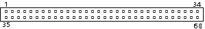
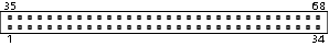
PC Card ATA bus pinout

bus or interface

bookmark this page

This specification makes it possible to share ATA & PC Card with the same connectors.

68 pin male connector layout

68 pin male connector
at the controller


Pin Namel Host Dir Dev PC-Card equiv
1Groundx-->xGround
2DD3x<->xD3
3DD4x<->xD4
4DD5x<->xD5
5DD6x<->xD6
6DD7x<->xD7
7/CS0x-->x/CE1
8  -->iA10
9/SELATAx-->x/OE
10     
11/CS1x-->x 1)A9
12  -->iA8
13     
14     
15  -->i/WE
16INTRQx<--x/READY:IREQ
17VCCx-->xVCC
18     
19     
20     
21     
22  -->iA7
23  -->iA6
24  -->iA5
25  -->iA4
26  -->iA3
27DA2x-->xA2
28DA1x-->xA1
29DA0x-->xA0
30DD0x<->xD0
31DD1x<->xD1
32DD2x<->xD2
33/IOCS16x<--x/WP:IOIS16
34Groundx-->xGround
35Groundx-->xGround
36/CD1x<--x/CD1
37DD11x<->xD11
38DD12x<->xD12
39DD13x<->xD13
40DD14x<->xD14
41DD15x<->xD15
42/CS1x-->x 1)/CE2
43  <--i/VS1
44/DIORx-->x/IORD
45/DIOWx-->x/IOWR
46     
47     
48     
49     
50     
51VCCx-->xVCC
52     
53     
54     
55M/S-x-->x 2) 
56CSELx-->x 2) 
57  <--i/VS2
58/RESETx-->xRESET
59IORDYo<--x 3)/WAIT
60DMARQo<--x 3)/INPACK
61/DMACKo-->o/REG
62/DASPx<->x/BVD2:SPKR
63/PDIAGx<->x/BVD1:STSCHG
64DD8x<->xD8
65DD9x<->xD9
66DD10x<->xD10
67/CD2x<--x/CD2
68Groundx-->xGround
x = Required.
i = Ignored by host in ATA mode.
o = Optional.
nothing = Not connected.
1) Device shall support only one /CS1 signal pin.
2) Device shall support either /M/S or CSEL but not both.
3)


This information should be correct, but may be not. Please, help us to improve this document!
Is this document CORRECT or INCORRECT? Your opinion will be used to establish document status (showed at the bottom).
68 pin female connector diagram

68 pin female connector
at the peripherals

Pinouts.ru > Buses and slots connectors pinouts >  Pinout of PC Card ATA bus and layout of 68 pin male connector and 68 pin female connector
Document status: unknown
Source(s) of this and additional information: ATA-2 specifications, from Hardware Book 0 reports
Last updated at Sat Jun 25 2005. Submit additions or corrections for this document. Is this document correct or incorrect? What is your opinion?
[Discuss at the forum] [Back to index] [SUBMIT new pinout]
This page contain parts under Copyright © 2000-2007 by pinouts.ru team.
No any portion of this webpage may be reproduced in any form without visible direct link to this page provided. Webmaster permission required in any other cases.
Efforts have been made to ensure this page is correct, but it is the responsibility of the user to verify the data is correct for their application.
10330 hits since March 4, 2005