CompactPCI is an adaptation of the Peripheral Component Interconnect (PCI) Specification for industrial and/or embedded applications requiring a more robust mechanical form factor than desktop PCI. CompactPCI uses industry standard mechanical components and high-performance connector technologies to provide a system optimized for rugged applications. cPCI is electrically identical to the PCI specification (except it uses the Euro (VME) card 3U/6U format with 2mm connectors), allowing low-cost PCI chipsets to be utilized in a mechanical form factor suited for rugged environments. The cPCI bus uses 8, 16, 32, or 64 bit transfers with up to 532MBps. The CompactPCI specification accommodates a methodology for live insertion and removal of adapters. 3U CompactPCI boards use a single 220 pin connector for all power, ground, and all 32 and 64 bit PCI signals. This connector is called J1. Twenty pins are reserved for future use. Backplanes use male (pin) connectors and plug-in boards use female (socket) connectors. Plug in boards that only perform 32 bit transfers can use a smaller 110 pin connector. 32 bit boards and 64 bit boards can be intermixed and plugged into a single 64 bit backplane. 6U boards have an additional 220 pin connector. This connector is intentionally undefined at this time. It is used for a variety of purposes. It can be used as a bridge to other buses like VME or ISA. These "hybrid" backplanes use CompactPCI for the processor and high speed peripheral section and one of these industrial buses for an I/O expansion section. Overview:A CompactPCI system is composed of up to eight CompactPCI card locations: - One System Slot
- Up to seven Peripheral Slots
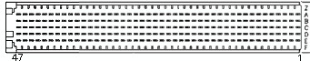
The connector has 7 columns with 47 rows. Normally the outside ground rows "Z" and "F" are not counted as pins. Pins are divided into groups: - Row 1-25: 32-bit PCI
- Row 26-47: Additional pins for 64-bit PCI (System Slot boards must use it).
- Row 26-28 and 40-42: Primarily implemented on System Slot boards.
Connector:| 1 | GND | 5V | -12V | TRST# | 12V | 5V | GND |
|---|
| 2 | GND | TCK | 5V | TMS | DO | TDI | GND |
|---|
| 3 | GND | INTA# | INTB# | INTC# | 5V | INTD# | GND |
|---|
| 4 | GND | BRSV | GND | V(I/O) | INTP | INTS | GND |
|---|
| 5 | GND | BRSV | BRSV | RST | GND | GNT# | GND |
|---|
| 6 | GND | REQ# | GND | 3.3V | CLK | AD(31) | GND |
|---|
| 7 | GND | AD(30) | AD(29) | AD(28) | GND | AD(27) | GND |
|---|
| 8 | GND | AD(26) | GND | V(I/O) | AD(25) | AD(24) | GND |
|---|
| 9 | GND | C/BE(3)# | IDSEL | AD(23) | GND | AD(22) | GND |
|---|
| 10 | GND | AD(21) | GND | 3.3V | AD(20) | AD(19) | GND |
|---|
| 11 | GND | AD(18) | AS(17) | AD(16) | GND | C/BE(2)# | GND |
|---|
| 12 | KEY | KEY | KEY | KEY | KEY | KEY | KEY |
|---|
| 13 | KEY | KEY | KEY | KEY | KEY | KEY | KEY |
|---|
| 14 | KEY | KEY | KEY | KEY | KEY | KEY | KEY |
|---|
| 15 | GND | 3.3V | FRAME# | IRDY# | GND | TRDY# | GND |
|---|
| 16 | GND | DEVSEL# | GND | V(I/O) | STOP# | LOCK# | GND |
|---|
| 17 | GND | 3.3V | SDONE | SBO# | GND | PERR# | GND |
|---|
| 18 | GND | SERR# | GND | 3.3V | PAR | C/BE(1)# | GND |
|---|
| 19 | GND | 3.3V | AD(15) | AD(14) | GND | AD(13) | GND |
|---|
| 20 | GND | AD(12) | GND | V(I/O) | AD(11) | AD(10) | GND |
|---|
| 21 | GND | 3.3V | AD(9) | AD(8) | M66EN | C/BE(0)# | GND |
|---|
| 22 | GND | AD(7) | GND | 3.3V | AD(6) | AD(5) | GND |
|---|
| 23 | GND | 3.3V | AD(4) | AD(3) | 5V | AD(2) | GND |
|---|
| 24 | GND | AD(1) | 5V | V(I/O) | AD(0) | ACK64# | GND |
|---|
| 25 | GND | 5V | REQ64# | BRSV | 3.3V | 5V | GND |
|---|
| 26 | GND | CLK1 | GND | REQ1# | GNT1# | REQ2# | GND |
|---|
| 27 | GND | CLK2 | CLK3 | SYSEN# | GNT2# | REQ3# | GND |
|---|
| 28 | GND | CLK4 | GND | GNT3# | REQ4# | GNT4# | GND |
|---|
| 29 | GND | V(I/O) | BRSV | C/BE(7 ) | GND | C/BE(6)# | GND |
|---|
| 30 | GND | C/BE(5)# | GND | V(I/O) | C/BE(4)# | PAR64 | GND |
|---|
| 31 | GND | AD(63) | AD(62) | AD(61) | GND | AD(60) | GND |
|---|
| 32 | GND | AD(59) | GND | V(I/O) | AD(58) | AD(57) | GND |
|---|
| 33 | GND | AD(56) | AD(55) | AD(54) | GND | AD(53) | GND |
|---|
| 34 | GND | AD(52) | GND | V(I/O) | AD(51) | AD(50) | GND |
|---|
| 35 | GND | AD(49) | AD(48) | AD(47) | GND | AD(46) | GND |
|---|
| 36 | GND | AD(45) | GND | V(I/O) | AD(44) | AD(43) | GND |
|---|
| 37 | GND | AD(42) | AD(41) | AD(40) | GND | AD(39) | GND |
|---|
| 38 | GND | AD(38) | GND | V(I/O) | AD(37) | AD(36) | GND |
|---|
| 39 | GND | AD(35) | AD(34) | AD(33) | GND | AD(32) | GND |
|---|
| 40 | GND | BRSV | GND | FAL# | REQ5# | GNT5# | GND |
|---|
| 41 | GND | BRSV | BRSV | DEG# | GND | BRSV | GND |
|---|
| 42 | GND | BRSV | GND | PRST# | REQ6# | GNT6# | GND |
|---|
| 43 | GND | USR | USR | USR | USR | USR | GND |
|---|
| 44 | GND | USR | USR | USR | USR | USR | GND |
|---|
| 45 | GND | USR | USR | USR | USR | USR | GND |
|---|
| 46 | GND | USR | USR | USR | USR | USR | GND |
|---|
| 47 | GND | USR | USR | USR | USR | USR | GND |
|---|
| Z |
A |
B |
C |
D |
E |
F |
|---|
Same with short descriptions:| Pin | Name | Description |
|---|
| Z1 | GND | Ground |
| Z2 | GND | Ground |
| Z3 | GND | Ground |
| Z4 | GND | Ground |
| Z5 | GND | Ground |
| Z6 | GND | Ground |
| Z7 | GND | Ground |
| Z8 | GND | Ground |
| Z9 | GND | Ground |
| Z10 | GND | Ground |
| Z11 | GND | Ground |
| Z12 | KEY | Keyed (no pin) |
| Z13 | KEY | Keyed (no pin) |
| Z14 | KEY | Keyed (no pin) |
| Z15 | GND | Ground |
| Z16 | GND | Ground |
| Z17 | GND | Ground |
| Z18 | GND | Ground |
| Z19 | GND | Ground |
| Z20 | GND | Ground |
| Z21 | GND | Ground |
| Z22 | GND | Ground |
| Z23 | GND | Ground |
| Z24 | GND | Ground |
| Z25 | GND | Ground |
| Z26 | GND | Ground |
| Z27 | GND | Ground |
| Z28 | GND | Ground |
| Z29 | GND | Ground |
| Z30 | GND | Ground |
| Z31 | GND | Ground |
| Z32 | GND | Ground |
| Z33 | GND | Ground |
| Z34 | GND | Ground |
| Z35 | GND | Ground |
| Z36 | GND | Ground |
| Z37 | GND | Ground |
| Z38 | GND | Ground |
| Z39 | GND | Ground |
| Z40 | GND | Ground |
| Z41 | GND | Ground |
| Z42 | GND | Ground |
| Z43 | GND | Ground |
| Z44 | GND | Ground |
| Z45 | GND | Ground |
| Z46 | GND | Ground |
| Z47 | GND | Ground |
| | |
| A1 | 5V | +5 VDC |
| A2 | TCK | Test Clock |
| A3 | INTA# | Interrupt A |
| A4 | BRSV | Bused Reserved (don"t use) |
| A5 | BRSV | Bused Reserved (don"t use) |
| A6 | REQ# | Request PCI transfer |
| A7 | AD(30) | Address/Data 30 |
| A8 | AD(26) | Address/Data 26 |
| A9 | C/BE(3)# | Command: Byte Enable |
| A10 | AD(21) | Address/Data 21 |
| A11 | AD(18) | Address/Data 18 |
| A12 | KEY | Keyed (no pin) |
| A13 | KEY | Keyed (no pin) |
| A14 | KEY | Keyed (no pin) |
| A15 | 3.3V | +3.3 VDC |
| A16 | DEVSEL# | Device Select |
| A17 | 3.3V | +3.3 VDC |
| A18 | SERR# | System Error |
| A19 | 3.3V | +3.3 VDC |
| A20 | AD(12) | Address/Data 12 |
| A21 | 3.3V | +3.3 VDC |
| A22 | AD(7) | Address/Data 7) |
| A23 | 3.3V | +3.3 VDC |
| A24 | AD(1) | Address/Data 1) |
| A25 | 5V | +5 VDC |
| A26 | CLK1 | Clock ?? MHz |
| A27 | CLK2 | Clock ?? MHz |
| A28 | CLK4 | Clock ?? MHz |
| A29 | V(I/O) | +3.3 VDC or +5 VDC |
| A30 | C/BE(5)# | Command: Byte Enable |
| A31 | AD(63) | Address/Data 63 |
| A32 | AD(59) | Address/Data 59 |
| A33 | AD(56) | Address/Data 56 |
| A34 | AD(52) | Address/Data 52 |
| A35 | AD(49) | Address/Data 49 |
| A36 | AD(45) | Address/Data 45 |
| A37 | AD(42) | Address/Data 42 |
| A38 | AD(38) | Address/Data 38 |
| A39 | AD(35) | Address/Data 35 |
| A40 | BRSV | Bused Reserved (don"t use) |
| A41 | BRSV | Bused Reserved (don"t use) |
| A42 | BRSV | Bused Reserved (don"t use) |
| A43 | USR | User Defined |
| A44 | USR | User Defined |
| A45 | USR | User Defined |
| A46 | USR | User Defined |
| A47 | USR | User Defined |
| | |
| B1 | -12V | -12 VDC |
| B2 | 5V | +5 VDC |
| B3 | INTB# | Interrupt B |
| B4 | GND | Ground |
| B5 | BRSV | Bused Reserved (don"t use) |
| B6 | GND | Ground |
| B7 | AD(29) | Address/Data 29 |
| B8 | GND | Ground |
| B9 | IDSEL | Initialization Device Select |
| B10 | GND | Ground |
| B11 | AD(17) | Address/Data 17 |
| B12 | KEY | Keyed (no pin) |
| B13 | KEY | Keyed (no pin) |
| B14 | KEY | Keyed (no pin) |
| B15 | FRAME# | Address or Data phase |
| B16 | GND | Ground |
| B17 | SDONE | Snoop Done |
| B18 | GND | Ground |
| B19 | AD(15) | Address/Data 15 |
| B20 | GND | Ground |
| B21 | AD(9) | Address/Data 9) |
| B22 | GND | Ground |
| B23 | AD(4) | Address/Data 4) |
| B24 | 5V | +5 VDC |
| B25 | REQ64# | |
| B26 | GND | Ground |
| B27 | CLK3 | Clock ?? MHz |
| B28 | GND | Ground |
| B29 | BRSV | Bused Reserved (don"t use) |
| B30 | GND | Ground |
| B31 | AD(62) | Address/Data 62 |
| B32 | GND | Ground |
| B33 | AD(55) | Address/Data 55 |
| B34 | GND | Ground |
| B35 | AD(48) | Address/Data 48 |
| B36 | GND | Ground |
| B37 | AD(41) | Address/Data 41 |
| B38 | GND | Ground |
| B39 | AD(34) | Address/Data 34 |
| B40 | GND | Ground |
| B41 | BRSV | Bused Reserved (don"t use) |
| B42 | GND | Ground |
| B43 | USR | User Defined |
| B44 | USR | User Defined |
| B45 | USR | User Defined |
| B46 | USR | User Defined |
| B47 | USR | User Defined |
| | |
| C1 | TRST# | Test Logic Reset |
| C2 | TMS | Test Mode Select |
| C3 | INTC# | Interrupt C |
| C4 | V(I/O) | +3.3 VDC or +5 VDC |
| C5 | RST | Reset |
| C6 | 3.3V | +3.3 VDC |
| C7 | AD(28) | Address/Data 28 |
| C8 | V(I/O) | +3.3 VDC or +5 VDC |
| C9 | AD(23) | Address/Data 23 |
| C10 | 3.3V | +3.3 VDC |
| C11 | AD(16) | Address/Data 16 |
| C12 | KEY | Keyed (no pin) |
| C13 | KEY | Keyed (no pin) |
| C14 | KEY | Keyed (no pin) |
| C15 | IRDY# | Initiator Ready |
| C16 | V(I/O) | +3.3 VDC or +5 VDC |
| C17 | SBO# | Snoop Backoff |
| C18 | 3.3V | +3.3 VDC |
| C19 | AD(14) | Address/Data 14 |
| C20 | V(I/O) | +3.3 VDC or +5 VDC |
| C21 | AD(8) | Address/Data 8) |
| C22 | 3.3V | +3.3 VDC |
| C23 | AD(3) | Address/Data 3) |
| C24 | V(I/O) | +3.3 VDC or +5 VDC |
| C25 | BRSV | Bused Reserved (don"t use) |
| C26 | REQ1# | Request PCI transfer |
| C27 | SYSEN# | |
| C28 | GNT3# | Grant |
| C29 | C/BE(7) | Command: Byte Enable |
| C30 | V(I/O) | +3.3 VDC or +5 VDC |
| C31 | AD(61) | Address/Data 61 |
| C32 | V(I/O) | +3.3 VDC or +5 VDC |
| C33 | AD(54) | Address/Data 54 |
| C34 | V(I/O) | +3.3 VDC or +5 VDC |
| C35 | AD(47) | Address/Data 47 |
| C36 | V(I/O) | +3.3 VDC or +5 VDC |
| C37 | AD(40) | Address/Data 40 |
| C38 | V(I/O) | +3.3 VDC or +5 VDC |
| C39 | AD(33) | Address/Data 33 |
| C40 | FAL# | Power Supply Status FAL (CompactPCI specific) |
| C41 | DEG# | Power Supply Status DEG (CompactPCI specific) |
| C42 | PRST# | Push Button Reset (CompactPCI specific) |
| C43 | USR | User Defined |
| C44 | USR | User Defined |
| C45 | USR | User Defined |
| C46 | USR | User Defined |
| C47 | USR | User Defined |
| | |
| D1 | +12V | +12 VDC |
| D2 | TDO | Test Data Output |
| D3 | 5V | +5 VDC |
| D4 | INTP | |
| D5 | GND | Ground |
| D6 | CLK | |
| D7 | GND | Ground |
| D8 | AD(25) | Address/Data 25 |
| D9 | GND | Ground |
| D10 | AD(20) | Address/Data 20 |
| D11 | GND | Ground |
| D12 | KEY | Keyed (no pin) |
| D13 | KEY | Keyed (no pin) |
| D14 | KEY | Keyed (no pin) |
| D15 | GND | Ground |
| D16 | STOP# | Stop transfer cycle |
| D17 | GND | Ground |
| D18 | PAR | Parity for AD0-31 & C/BE0-3 |
| D19 | GND | Ground |
| D20 | AD(11) | Address/Data 11 |
| D21 | M66EN | |
| D22 | AD(6) | Address/Data 6) |
| D23 | 5V | +5 VDC |
| D24 | AD(0) | Address/Data 0) |
| D25 | 3.3V | +3.3 VDC |
| D26 | GNT1# | Grant |
| D27 | GNT2# | Grant |
| D28 | REQ4# | Request PCI transfer |
| D29 | GND | Ground |
| D30 | C/BE(4)# | Command: Byte Enable |
| D31 | GND | Ground |
| D32 | AD(58) | Address/Data 58 |
| D33 | GND | Ground |
| D34 | AD(51) | Address/Data 51 |
| D35 | GND | Ground |
| D36 | AD(44) | Address/Data 44 |
| D37 | GND | Ground |
| D38 | AD(37) | Address/Data 37 |
| D39 | GND | Ground |
| D40 | REQ5# | Request PCI transfer |
| D41 | GND | Ground |
| D42 | REQ6# | Request PCI transfer |
| D43 | USR | User Defined |
| D44 | USR | User Defined |
| D45 | USR | User Defined |
| D46 | USR | User Defined |
| D47 | USR | User Defined |
| | |
| E1 | 5V | +5 VDC |
| E2 | TDI | Test Data Input |
| E3 | INTD# | Interrupt D |
| E4 | INTS | |
| E5 | GNT# | Grant |
| E6 | AD(31) | Address/Data 31 |
| E7 | AD(27) | Address/Data 27 |
| E8 | AD(24) | Address/Data 24 |
| E9 | AD(22) | Address/Data 22 |
| E10 | AD(19) | Address/Data 19 |
| E11 | C/BE(2)# | Command: Byte Enable |
| E12 | KEY | Keyed (no pin) |
| E13 | KEY | Keyed (no pin) |
| E14 | KEY | Keyed (no pin) |
| E15 | TRDY# | Target Ready |
| E16 | LOCK# | Lock resource |
| E17 | PERR# | Parity Error |
| E18 | C/BE(1)# | Command: Byte Enable |
| E19 | AD(13) | Address/Data 13 |
| E20 | AD(10) | Address/Data 10 |
| E21 | C/BE(0)# | Command: Byte Enable |
| E22 | AD(5) | Address/Data 5) |
| E23 | AD(2) | Address/Data 2) |
| E24 | ACK64# | |
| E25 | 5V | +5 VDC |
| E26 | REQ2# | Request PCI transfer |
| E27 | REQ3# | Request PCI transfer |
| E28 | GNT4# | Grant |
| E29 | C/BE(6)# | Command: Byte Enable |
| E30 | PAR64 | |
| E31 | AD(60) | Address/Data 60 |
| E32 | AD(57) | Address/Data 57 |
| E33 | AD(53) | Address/Data 53 |
| E34 | AD(50) | Address/Data 50 |
| E35 | AD(46) | Address/Data 46 |
| E36 | AD(43) | Address/Data 43 |
| E37 | AD(39) | Address/Data 39 |
| E38 | AD(36) | Address/Data 36 |
| E39 | AD(32) | Address/Data 32 |
| E40 | GNT5# | Grant |
| E41 | BRSV | Bused Reserved (don"t use) |
| E42 | GNT6# | Grant |
| E43 | USR | User Defined |
| E44 | USR | User Defined |
| E45 | USR | User Defined |
| E46 | USR | User Defined |
| E47 | USR | User Defined |
| | |
| F1 | GND | Ground |
| F2 | GND | Ground |
| F3 | GND | Ground |
| F4 | GND | Ground |
| F5 | GND | Ground |
| F6 | GND | Ground |
| F7 | GND | Ground |
| F8 | GND | Ground |
| F9 | GND | Ground |
| F10 | GND | Ground |
| F11 | GND | Ground |
| F12 | KEY | Keyed (no pin) |
| F13 | KEY | Keyed (no pin) |
| F14 | KEY | Keyed (no pin) |
| F15 | GND | Ground |
| F16 | GND | Ground |
| F17 | GND | Ground |
| F18 | GND | Ground |
| F19 | GND | Ground |
| F20 | GND | Ground |
| F21 | GND | Ground |
| F22 | GND | Ground |
| F23 | GND | Ground |
| F24 | GND | Ground |
| F25 | GND | Ground |
| F26 | GND | Ground |
| F27 | GND | Ground |
| F28 | GND | Ground |
| F29 | GND | Ground |
| F30 | GND | Ground |
| F31 | GND | Ground |
| F32 | GND | Ground |
| F33 | GND | Ground |
| F34 | GND | Ground |
| F35 | GND | Ground |
| F36 | GND | Ground |
| F37 | GND | Ground |
| F38 | GND | Ground |
| F39 | GND | Ground |
| F40 | GND | Ground |
| F41 | GND | Ground |
| F42 | GND | Ground |
| F43 | GND | Ground |
| F44 | GND | Ground |
| F45 | GND | Ground |
| F46 | GND | Ground |
| F47 | GND | Ground |
Signal Descriptions: PRSTPush Button Reset. DEGPower Supply Status DEG FALPower Supply Status FAL SYSENSystem Slot Identification The following signals must be terminated: - AD0-31
- C/BE0#-C/BE3#
- PAR
- FRAME#
- IRDY#
- TRDY#
- STOP#
- LOCK#
- IDSEL
- DEVSEL#
- PERR#
- SERR#
- RST#
The following signals must be terminated if used: - INTA#
- INTB#
- INTC#
- INTD#
- SB0#
- SDOBE
- AD32-AD63
- C/BE4#-C/BE7#
- REQ64#
- ACK64#
- PAR64#
The following signals do no require a stub termination: - CLK
- REQ#
- GNT#
- TDI#
- TDO
- TCK
- TMS
- TRST#
The System Slot board must pullup the following signals (even if not used): For a copy of the full CompactPCI standard, contact: PCI Industrial Computer Manufacturers Group (PICMG)
c/o Roger Communications
301 Edgewater place
Suite 220
Wakewater
MA01880
Phone: 1-617-224-1100
Fax: 1-617-224-1239
This information should be correct, but may be not. Please, help us to improve this document!
Is this document CORRECT or INCORRECT? Your opinion will be used to establish document status (showed at the bottom). |
|