|
60 Pin1 |
Signal |
25 Pin |
Signal | Direction
DTE DCE2 |
|---|
J1-11
J1-12 | TxD/RxD+
TxD/RxD- | J2-2
J2-14 | BA(A), TxD+
BA(B), TxD- | 
|
J1-28
J1-27 | RxD/TxD+
RxD/TxD- | J2-3
J2-16 | BB(A), RxD+
BB(B), RxD- | 
|
J1-9
J1-10 | RTS/CTS+
RTS/CTS- | J2-4
J2-19 | CA(A), RTS+
CA(B), RTS- |
|
J1-1
J1-2 | CTS/RTS+
CTS/RTS- | J2-5
J2-13 | CB(A), CTS+
CB(B), CTS- |
|
J1-3
J1-4 | DSR/DTR+
DSR/DTR- | J2-6
J2-22 | CC(A), DSR+
CC(B), DSR- |
|
J1-46
J1-47 | Shield_GND
MODE_2 | J2-1
- | Shield
- | Shorted |
J1-48
J1-49 | GND
MODE_1 | -
- | -
- | Shorted |
J1-5
J1-6 | DCD/DCD+
DCD/DCD- | J2-8
J2-10 | CF(A), DCD+
CF(B), DCD- |
|
J1-24
J1-23 | TxC/RxC+
TxC/RxC- | J2-15
J2-12 | DB(A), TxC+
DB(B), TxC- |
|
J1-26
J1-25 | RxC/TxCE+
RxC/TxCE- | J2-17
J2-9 | DD(A), RxC+
DD(B), RxC- |
|
J1-44
J1-45 | LL/DCD
Circuit_GND | J2-18
J2-7 | LL
Circuit_ GND |
- |
J1-7
J1-8 | DTR/DSR+
DTR/DSR- | J2-20
J2-23 | CD(A), DTR+
CD(B), DTR- |
|
J1-13
J1-14 | TxCE/TxC+
TxCE/TxC- | J2-24
J2-11 | DA(A), TxCE+
DA(B), TxCE- |
|
Arrows indicate signal direction:
indicates DTE to DCE, and
indicates DCE to DTE. 1
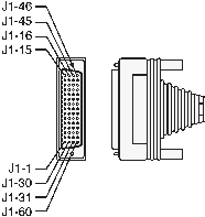
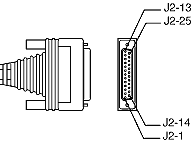
Any pin not referenced is not connected.
2
The EIA-530 interface cannot be operated in DCE mode. A DCE cable is not available for the EIA-530 interface.
This information should be correct, but may be not. Please, help us to improve this document!
Is this document CORRECT or INCORRECT? Your opinion will be used to establish document status (showed at the bottom). |
| |