Hardware pinouts information and cables schemes

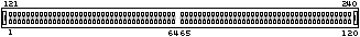
DDR2 DIMM Unbuffered Module (240 pin) pinout

memory connector

bookmark this page

240 pin DIMM DDR2 connector layout

240 pin DIMM DDR2 connector
at the motheboard


Pin # Description Pin # Description
1VREF121VSS
2VSS122DQ4
3DQ0123DQ5
4DQ1124VSS
5VSS125DM0
6/DQS0126NC
7DQS0127VSS
8VSS128DQ6
9DQ2129DQ7
10DQ3130VSS
11VSS131DQ12
12DQ8132DQ13
13DQ9133VSS
14VSS134DM1
15/DQS1135NC
16DQS1136VSS
17VSS137CK1
18NC138/CK1
19NC139VSS
20VSS140DQ14
21DQ10141DQ15
22DQ11142VSS
23VSS143DQ20
24DQ16144DQ21
25DQ17145VSS
26VSS146DM2
27/DQS2147NC
28DQS2148VSS
29VSS149DQ22
30DQ18150DQ23
31DQ19151VSS
32VSS152DQ28
33DQ24153DQ29
34DQ25154VSS
35VSS155DM3
36/DQS3156NC
37DQS3157VSS
38VSS158DQ30
39DQ26159DQ31
40DQ27160VSS
41VSS161NC
42NC162NC
43NC163VSS
44VSS164NC
45NC165NC
46NC166VSS
47VSS167NC
48NC168NC
49NC169VSS
50VSS170VDDQ
51VDDQ171CKE1
52CKE0172VDD
53VDD173NC
54NC174NC
55NC175VDDQ
56VDDQ176A12
57A11177A9
58A7178VDD
59VDD179A8
60A5180A6
61A4181VDDQ
62VDDQ182A3
63A2183A1
64VDD184VDD
KEY
65VSS185CK0
66VSS186/CK0
67VDD187VDD
68NC188A0
69VDD189VDD
70A10/AP190BA1
71BA0191VDDQ
72VDDQ192/RAS
73/WE193/CS0
74/CAS194VDDQ
75VDDQ195ODT0
76/CS1196A13
77ODT1197VDD
78VDDQ198VSS
79VSS199DQ36
80DQ32200DQ37
81DQ33201VSS
82VSS202DM4
83/DQS4203NC
84DQS4204VSS
85VSS205DQ38
86DQ34206DQ39
87DQ35207VSS
88VSS208DQ44
89DQ40209DQ45
90DQ41210VSS
91VSS211DM5
92/DQS5212NC
93DQS5213VSS
94VSS214DQ46
95DQ42215DQ47
96DQ43216VSS
97VSS217DQ52
98DQ48218DQ53
99DQ49219VSS
100VSS220CK2
101SA2221/CK2
102NC222VSS
103VSS223DM6
104/DQS6224NC
105DQS6225VSS
106VSS226DQ54
107DQ50227DQ55
108DQ51228VSS
109VSS229DQ60
110DQ56230DQ61
111DQ57231VSS
112VSS232DM7
113/DQS7233NC
114DQS7234VSS
115VSS235DQ62
116DQ58236DQ63
117DQ59237VSS
118VSS238VDDSPD
119SDA239SA0
120SCL240SA1

Some pins functions:

A0 to A13 Address input
BA0, BA1 Bank select address
DQ0 to DQ63 Data input/output
/RAS Row address strobe command
/CAS Column address strobe command
/WE Write enable
/CS0, /CS1 Chip select
CKE0, CKE1 Clock enable
CK0 to CK2 Clock input
/CK0 to /CK2 Differential clock input
DQS0 to DQS7, /DQS0 to /DQS7 Input and output data strobe
DM0 to DM7 Input mask
SCL Clock input for SPD
SDA Data input/output for SPD
SA0 to SA2 Serial address input
VDD Power for internal circuit
VDDQ Power for DQ circuit
VDDSPD Power for serial EEPROM
VREF Input reference voltage
VSS Ground
ODT0, ODT1 ODT control
NC No Connection


This information should be correct, but may be not. Please, help us to improve this document!
Is this document CORRECT or INCORRECT? Your opinion will be used to establish document status (showed at the bottom).
Pinouts.ru > Memory slots and cards connectors pinouts >  Pinout of DDR2 DIMM Unbuffered Module (240 pin) and layout of 240 pin DIMM DDR2 connector
Document status: unknown
1 reports
Last updated at Sat Aug 19 2006. Submit additions or corrections for this document. Is this document correct or incorrect? What is your opinion?
[Discuss at the forum] [Back to index] [SUBMIT new pinout]
This page contain parts under Copyright © 2000-2007 by pinouts.ru team.
No any portion of this webpage may be reproduced in any form without visible direct link to this page provided. Webmaster permission required in any other cases.
Efforts have been made to ensure this page is correct, but it is the responsibility of the user to verify the data is correct for their application.
16692 hits since March 4, 2005