|
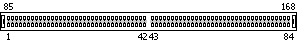
Front Side (left side 1-42, right side 43-84)
Back Side (left side 85-126, right side 127-168)
Front, Left| Pin | Non-Parity | 72 ECC? | 80 ECC? | Description |
|---|
| 1 | VSS | VSS | VSS | Ground |
| 2 | DQ0 | DQ0 | DQ0 | Data 0 |
| 3 | DQ1 | DQ1 | DQ1 | Data 1 |
| 4 | DQ2 | DQ2 | DQ2 | Data 2 |
| 5 | DQ3 | DQ3 | DQ3 | Data 3 |
| 6 | VDD | VDD | VDD | +5 VDC or +3.3 VDC |
| 7 | DQ4 | DQ4 | DQ4 | Data 4 |
| 8 | DQ5 | DQ5 | DQ5 | Data 5 |
| 9 | DQ6 | DQ6 | DQ6 | Data 6 |
| 10 | DQ7 | DQ7 | DQ7 | Data 7 |
| 11 | DQ8 | DQ8 | DQ8 | Data 8 |
| 12 | VSS | VSS | VSS | Ground |
| 13 | DQ9 | DQ9 | DQ9 | Data 9 |
| 14 | DQ10 | DQ10 | DQ10 | Data 10 |
| 15 | DQ11 | DQ11 | DQ11 | Data 11 |
| 16 | DQ12 | DQ12 | DQ12 | Data 12 |
| 17 | DQ13 | DQ13 | DQ13 | Data 13 |
| 18 | VDD | VDD | VDD | +5 VDC or +3.3 VDC |
| 19 | DQ14 | DQ14 | DQ14 | Data 14 |
| 20 | DQ15 | DQ15 | DQ15 | Data 15 |
| 21 | n/c | CB0 | CB0 | Parity/Check Bit Input/Output 0 |
| 22 | n/c | CB1 | CB1 | Parity/Check Bit Input/Output 01 |
| 23 | VSS | VSS | VSS | Ground |
| 24 | n/c | n/c | CB8 | Parity/Check Bit Input/Output 8 |
| 25 | n/c | n/c | CB9 | Parity/Check Bit Input/Output 9 |
| 26 | VDD | VDD | VDD | +5 VDC or +3.3 VDC |
| 27 | /WE | /WE | /WE | Read/Write |
| 28 | DQMB0 | DQMB0 | DQMB0 | Byte Mask signal 0 |
| 29 | DQMB1 | DQMB1 | DQMB1 | Byte Mask signal 1 |
| 30 | /S0 | /S0 | /S0 | Chip Select 0 |
| 31 | DU | DU | DU | Don't Use |
| 32 | VSS | VSS | VSS | Ground |
| 33 | A0 | A0 | A0 | Address 0 |
| 34 | A2 | A2 | A2 | Address 2 |
| 35 | A4 | A4 | A4 | Address 4 |
| 36 | A6 | A6 | A6 | Address 6 |
| 37 | A8 | A8 | A8 | Address 8 |
| 38 | A10/AP | A10/AP | A10/AP | Address 10 |
| 39 | BA1 | BA1 | BA1 | Bank Address 1 |
| 40 | VDD | VDD | VDD | +5 VDC or +3.3 VDC |
| 41 | VDD | VDD | VDD | +5 VDC or +3.3 VDC |
| 42 | CK0 | CK0 | CK0 | Clock signal 0 |
Front, Right| Pin | Non-Parity | 72 ECC? | 80 ECC? | Description |
|---|
| 43 | VSS | VSS | VSS | Ground |
| 44 | DU | DU | DU | Don't Use |
| 45 | /S2 | /S2 | /S2 | Chip Select 2 |
| 46 | DQMB2 | DQMB2 | DQMB2 | Byte Mask signal 2 |
| 47 | DQMB3 | DQMB3 | DQMB3 | Byte Mask signal 3 |
| 48 | DU | DU | DU | Don't Use |
| 49 | VDD | VDD | VDD | +5 VDC or +3.3 VDC |
| 50 | n/c | n/c | CB10 | Parity/Check Bit Input/Output 10 |
| 51 | n/c | n/c | CB11 | Parity/Check Bit Input/Output 11 |
| 52 | n/c | CB2 | CB2 | Parity/Check Bit Input/Output 2 |
| 53 | n/c | CB3 | CB3 | Parity/Check Bit Input/Output 3 |
| 54 | VSS | VSS | VSS | Ground |
| 55 | DQ16 | DQ16 | DQ16 | Data 16 |
| 56 | DQ17 | DQ17 | DQ17 | Data 17 |
| 57 | DQ18 | DQ18 | DQ18 | Data 18 |
| 58 | DQ19 | DQ19 | DQ19 | Data 19 |
| 59 | VDD | VDD | VDD | +5 VDC or +3.3 VDC |
| 60 | DQ20 | DQ20 | DQ20 | Data 20 |
| 61 | n/c | n/c | n/c | Not connected |
| 62 | Vref,NC | Vref,NC | Vref,NC | |
| 63 | CKE1 | CKE1 | CKE1 | Clock Enable Signal 1 |
| 64 | VSS | VSS | VSS | Ground |
| 65 | DQ21 | DQ21 | DQ21 | Data 21 |
| 66 | DQ22 | DQ22 | DQ22 | Data 22 |
| 67 | DQ23 | DQ23 | DQ23 | Data 23 |
| 68 | VSS | VSS | VSS | Ground |
| 69 | DQ24 | DQ24 | DQ24 | Data 24 |
| 70 | DQ25 | DQ25 | DQ25 | Data 25 |
| 71 | DQ26 | DQ26 | DQ26 | Data 26 |
| 72 | DQ27 | DQ27 | DQ27 | Data 27 |
| 73 | VDD | VDD | VDD | +5 VDC or +3.3 VDC |
| 74 | DQ28 | DQ28 | DQ28 | Data 28 |
| 75 | DQ29 | DQ29 | DQ29 | Data 29 |
| 76 | DQ30 | DQ30 | DQ30 | Data 30 |
| 77 | DQ31 | DQ31 | DQ31 | Data 31 |
| 78 | VSS | VSS | VSS | Ground |
| 79 | CK2 | CK2 | CK2 | Clock signal 2 |
| 80 | n/c | n/c | n/c | Not connected |
| 81 | n/c | n/c | n/c | Not connected |
| 82 | SDA | SDA | SDA | Serial Data |
| 83 | SCL | SCL | SCL | Serial Clock |
| 84 | VDD | VDD | VDD | +5 VDC or +3.3 VDC |
Back, Left| Pin | Non-Parity | 72 ECC? | 80 ECC? | Description |
|---|
| 85 | VSS | VSS | VSS | Ground |
| 86 | DQ32 | DQ32 | DQ32 | Data 32 |
| 87 | DQ33 | DQ33 | DQ33 | Data 33 |
| 88 | DQ34 | DQ34 | DQ34 | Data 34 |
| 89 | DQ35 | DQ35 | DQ35 | Data 35 |
| 90 | VDD | VDD | VDD | +5 VDC or +3.3 VDC |
| 91 | DQ36 | DQ36 | DQ36 | Data 36 |
| 92 | DQ37 | DQ37 | DQ37 | Data 37 |
| 93 | DQ38 | DQ38 | DQ38 | Data 38 |
| 94 | DQ39 | DQ39 | DQ39 | Data 39 |
| 95 | DQ40 | DQ40 | DQ40 | Data 40 |
| 96 | VSS | VSS | VSS | Ground |
| 97 | DQ41 | DQ41 | DQ41 | Data 41 |
| 98 | DQ42 | DQ42 | DQ42 | Data 42 |
| 99 | DQ43 | DQ43 | DQ43 | Data 43 |
| 100 | DQ44 | DQ44 | DQ44 | Data 44 |
| 101 | DQ45 | DQ45 | DQ45 | Data 45 |
| 102 | VDD | VDD | VDD | +5 VDC or +3.3 VDC |
| 103 | DQ46 | DQ46 | DQ46 | Data 46 |
| 104 | DQ47 | DQ47 | DQ47 | Data 47 |
| 105 | n/c | CB4 | CB4 | Parity/Check Bit Input/Output 4 |
| 106 | n/c | CB5 | CB5 | Parity/Check Bit Input/Output 5 |
| 107 | VSS | VSS | VSS | Ground |
| 108 | n/c | n/c | CB12 | Parity/Check Bit Input/Output 12 |
| 109 | n/c | n/c | CB13 | Parity/Check Bit Input/Output 13 |
| 110 | VDD | VDD | VDD | +5 VDC or +3.3 VDC |
| 111 | /CAS | /CAS | /CAS | Column Address Strobe |
| 112 | DQMB4 | DQMB4 | DQMB4 | Byte Mask signal 4 |
| 113 | DQMB5 | DQMB5 | DQMB5 | Byte Mask signal 5 |
| 114 | /S1 | /S1 | /S1 | Chip Select 1 |
| 115 | /RAS | /RAS | /RAS | Row Address Strobe |
| 116 | VSS | VSS | VSS | Ground |
| 117 | A1 | A1 | A1 | Address 1 |
| 118 | A3 | A3 | A3 | Address 3 |
| 119 | A5 | A5 | A5 | Address 5 |
| 120 | A7 | A7 | A7 | Address 7 |
| 121 | A9 | A9 | A9 | Address 9 |
| 122 | BA0 | BA0 | BA0 | Bank Address 0 |
| 123 | A11 | A11 | A11 | Address 11 |
| 124 | VDD | VDD | VDD | +5 VDC or +3.3 VDC |
| 125 | CK1 | CK1 | CK1 | Clock signal 1 |
| 126 | A12 | A12 | A12 | Address 12 |
Back, Right| Pin | Non-Parity | 72 ECC? | 80 ECC? | Description |
|---|
| 127 | VSS | VSS | VSS | Ground |
| 128 | CKE0 | CKE0 | CKE0 | Clock Enable Signal 0 |
| 129 | /S3 | /S3 | /S3 | Chip Select 3 |
| 130 | DQMB6 | DQMB6 | DQMB6 | Byte Mask signal 6 |
| 131 | DQMB7 | DQMB7 | DQMB7 | Byte Mask signal 7 |
| 132 | A13 | A13 | A13 | Address 13 |
| 133 | VDD | VDD | VDD | +5 VDC or +3.3 VDC |
| 134 | n/c | n/c | CB14 | Parity/Check Bit Input/Output 14 |
| 135 | n/c | n/c | CB15 | Parity/Check Bit Input/Output 15 |
| 136 | n/c | CB6 | CB6 | Parity/Check Bit Input/Output 6 |
| 137 | n/c | CB7 | CB7 | Parity/Check Bit Input/Output 7 |
| 138 | VSS | VSS | VSS | Ground |
| 139 | DQ48 | DQ48 | DQ48 | Data 48 |
| 140 | DQ49 | DQ49 | DQ49 | Data 49 |
| 141 | DQ50 | DQ50 | DQ50 | Data 50 |
| 142 | DQ51 | DQ51 | DQ51 | Data 51 |
| 143 | VDD | VDD | VDD | +5 VDC or +3.3 VDC |
| 144 | DQ52 | DQ52 | DQ52 | Data 52 |
| 145 | n/c | n/c | n/c | Not connected |
| 146 | Vref,NC | Vref,NC | Vref,NC | |
| 147 | n/c | n/c | n/c | Not connected |
| 148 | VSS | VSS | VSS | Ground |
| 149 | DQ53 | DQ53 | DQ53 | Data 53 |
| 150 | DQ54 | DQ54 | DQ54 | Data 54 |
| 151 | DQ55 | DQ55 | DQ55 | Data 55 |
| 152 | VSS | VSS | VSS | Ground |
| 153 | DQ56 | DQ56 | DQ56 | Data 56 |
| 154 | DQ57 | DQ57 | DQ57 | Data 57 |
| 155 | DQ58 | DQ58 | DQ58 | Data 58 |
| 156 | DQ59 | DQ59 | DQ59 | Data 59 |
| 157 | VDD | VDD | VDD | +5 VDC or +3.3 VDC |
| 158 | DQ60 | DQ60 | DQ60 | Data 60 |
| 159 | DQ61 | DQ61 | DQ61 | Data 61 |
| 160 | DQ62 | DQ62 | DQ62 | Data 62 |
| 161 | DQ63 | DQ63 | DQ63 | Data 63 |
| 162 | VSS | VSS | VSS | Ground |
| 163 | CK3 | CK3 | CK3 | Clock signal 3 |
| 164 | n/c | n/c | n/c | Not connected |
| 165 | SA0 | SA0 | SA0 | Serial address 0 |
| 166 | SA1 | SA1 | SA1 | Serial address 1 |
| 167 | SA2 | SA2 | SA2 | Serial address 2 |
| 168 | VDD | VDD | VDD | +5 VDC or +3.3 VDC |
This information should be correct, but may be not. Please, help us to improve this document!
Is this document CORRECT or INCORRECT? Your opinion will be used to establish document status (showed at the bottom). |
| |