Hardware pinouts information and cables schemes

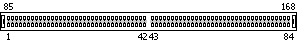
DRAM DIMM (168 pin, Unbuffered) pinout

memory connector

bookmark this page

DIMM=Dual Inline Memory Module

168 pin DIMM connector layout

168 pin DIMM connector
at the motherboard


Front Side (left side 1-42, right side 43-84)
Back Side (left side 85-126, right side 127-168)

Front, Left

Pin Non-Parity? Parity? 72 ECC? 80 ECC? Description
1VSSVSSVSSVSSGround
2DQ0DQ0DQ0DQ0Data 0
3DQ1DQ1DQ1DQ1Data 1
4DQ2DQ2DQ2DQ2Data 2
5DQ3DQ3DQ3DQ3Data 3
6VCCVCCVCCVCC+5 VDC or +3.3 VDC
7DQ4DQ4DQ4DQ4Data 4
8DQ5DQ5DQ5DQ5Data 5
9DQ6DQ6DQ6DQ6Data 6
10DQ7DQ7DQ7DQ7Data 7
11DQ8DQ8DQ8DQ8Data 8
12VSSVSSVSSVSSGround
13DQ9DQ9DQ9DQ9Data 9
14DQ10DQ10DQ10DQ10Data 10
15DQ11DQ11DQ11DQ11Data 11
16DQ12DQ12DQ12DQ12Data 12
17DQ13DQ13DQ13DQ13Data 13
18VCCVCCVCCVCC+5 VDC or +3.3 VDC
19DQ14DQ14DQ14DQ14Data 14
20DQ15DQ15DQ15DQ15Data 15
21n/cCB0CB0CB0Parity/Check Bit Input/Output 0
22n/cCB1CB1CB1Parity/Check Bit Input/Output 1
23VSSVSSVSSVSSGround
24n/cn/cn/cCB8Parity/Check Bit Input/Output 8
25n/cn/cn/cCB9Parity/Check Bit Input/Output 9
26VCCVCCVCCVCC+5 VDC or +3.3 VDC
27/WE0/WE0/WE0/WE0Read/Write Input
28/CAS0/CAS0/CAS0/CAS0Column Address Strobe 0
29/CAS1/CAS1/CAS1/CAS1Column Address Strobe 1
30/RAS0/RAS0/RAS0/RAS0Row Address Strobe 0
31/OE0/OE0/OE0/OE0Output Enable
32VSSVSSVSSVSSGround
33A0A0A0A0Address 0
34A2A2A2A2Address 2
35A4A4A4A4Address 4
36A6A6A6A6Address 6
37A8A8A8A8Address 8
38A10A10A10A10Address 10
39A12A12A12A12Address 12
40VCCVCCVCCVCC+5 VDC or +3.3 VDC
41VCCVCCVCCVCC+5 VDC or +3.3 VDC
42DUDUDUDUDon't Use

Front, Right

Pin Non-Parity? Parity? 72 ECC? 80 ECC? Description
43VSSVSSVSSVSSGround
44/OE2/OE2/OE2/OE2 
45/RAS2/RAS2/RAS2/RAS2Row Address Strobe 2
46/CAS2/CAS2/CAS2/CAS2Column Address Strobe 2
47/CAS3/CAS3/CAS3/CAS3Column Address Strobe 3
48/WE2/WE2/WE2/WE2Read/Write Input
49VCCVCCVCCVCC+5 VDC or +3.3 VDC
50n/cn/cn/cCB10Parity/Check Bit Input/Output 10
51n/cn/cn/cCB11Parity/Check Bit Input/Output 11
52n/cCB2CB2CB2Parity/Check Bit Input/Output 2
53n/cCB3CB3CB3Parity/Check Bit Input/Output 3
54VSSVSSVSSVSSGround
55DQ16DQ16DQ16DQ16Data 16
56DQ17DQ17DQ17DQ17Data 17
57DQ18DQ18DQ18DQ18Data 18
58DQ19DQ19DQ19DQ19Data 19
59VCCVCCVCCVCC+5 VDC or +3.3 VDC
60DQ20DQ20DQ20DQ20Data 20
61n/cn/cn/cn/cNot connected
62DUDUDUDUDon't Use
63n/cn/cn/cn/cNot connected
64VSSVSSVSSVSSGround
65DQ21DQ21DQ21DQ21Data 21
66DQ22DQ22DQ22DQ22Data 22
67DQ23DQ23DQ23DQ23Data 23
68VSSVSSVSSVSSGround
69DQ24DQ24DQ24DQ24Data 24
70DQ25DQ25DQ25DQ25Data 25
71DQ26DQ26DQ26DQ26Data 26
72DQ27DQ27DQ27DQ27Data 27
73VCCVCCVCCVCC+5 VDC or +3.3 VDC
74DQ28DQ28DQ28DQ28Data 28
75DQ29DQ29DQ29DQ29Data 29
76DQ30DQ30DQ30DQ30Data 30
77DQ31DQ31DQ31DQ31Data 31
78VSSVSSVSSVSSGround
79n/cn/cn/cn/cNot connected
80n/cn/cn/cn/cNot connected
81n/cn/cn/cn/cNot connected
82SDASDASDASDASerial Data
83SCLSCLSCLSCLSerial Clock
84VCCVCCVCCVCC+5 VDC or +3.3 VDC

Back, Left

Pin Non-Parity? Parity? 72 ECC? 80 ECC? Description
85VSSVSSVSSVSSGround
86DQ32DQ32DQ32DQ32Data 32
87DQ33DQ33DQ33DQ33Data 33
88DQ34DQ34DQ34DQ34Data 34
89DQ35DQ35DQ35DQ35Data 35
90VCCVCCVCCVCC+5 VDC or +3.3 VDC
91DQ36DQ36DQ36DQ36Data 36
92DQ37DQ37DQ37DQ37Data 37
93DQ38DQ38DQ38DQ38Data 38
94DQ39DQ39DQ39DQ39Data 39
95DQ40DQ40DQ40DQ40Data 40
96VSSVSSVSSVSSGround
97DQ41DQ41DQ41DQ41Data 41
98DQ42DQ42DQ42DQ42Data 42
99DQ43DQ43DQ43DQ43Data 43
100DQ44DQ44DQ44DQ44Data 44
101DQ45DQ45DQ45DQ45Data 45
102VCCVCCVCCVCC+5 VDC or +3.3 VDC
103DQ46DQ46DQ46DQ46Data 46
104DQ47DQ47DQ47DQ47Data 47
105n/cCB4CB4CB4Parity/Check Bit Input/Output 4
106n/cCB5CB5CB5Parity/Check Bit Input/Output 5
107VSSVSSVSSVSSGround
108n/cn/cn/cCB12Parity/Check Bit Input/Output 12
109n/cn/cn/cCB13Parity/Check Bit Input/Output 13
110VCCVCCVCCVCC+5 VDC or +3.3 VDC
111DUDUDUDUDon't Use
112/CAS4/CAS4/CAS4/CAS4Column Address Strobe 4
113/CAS5/CAS5/CAS5/CAS5Column Address Strobe 5
114/RAS1/RAS1/RAS1/RAS1Row Address Strobe 1
115DUDUDUDUDon't Use
116VSSVSSVSSVSSGround
117A1A1A1A1Address 1
118A3A3A3A3Address 3
119A5A5A5A5Address 5
120A7A7A7A7Address 7
121A9A9A9A9Address 9
122A11A11A11A11Address 11
123A13A13A13A13Address 13
124VCCVCCVCCVCC+5 VDC or +3.3 VDC
125DUDUDUDUDon't Use
126DUDUDUDUDon't Use

Back, Right

Pin Non-Parity? Parity? 72 ECC? 80 ECC? Description
127VSSVSSVSSVSSGround
128DUDUDUDUDon't Use
129/RAS3/RAS3/RAS3/RAS3Column Address Strobe 3
130/CAS6/CAS6/CAS6/CAS6Column Address Strobe 6
131/CAS7/CAS7/CAS7/CAS7Column Address Strobe 7
132DUDUDUDUDon't Use
133VCCVCCVCCVCC+5 VDC or +3.3 VDC
134n/cn/cn/cCB14Parity/Check Bit Input/Output 14
135n/cn/cn/cCB15Parity/Check Bit Input/Output 15
136n/cCB6CB6CB6Parity/Check Bit Input/Output 6
137n/cCB7CB7CB7Parity/Check Bit Input/Output 7
138VSSVSSVSSVSSGround
139DQ48DQ48DQ48DQ48Data 48
140DQ49DQ49DQ49DQ49Data 49
141DQ50DQ50DQ50DQ50Data 50
142DQ51DQ51DQ51DQ51Data 51
143VCCVCCVCCVCC+5 VDC or +3.3 VDC
144DQ52DQ52DQ52DQ52Data 52
145n/cn/cn/cn/cNot connected
146DUDUDUDUDon't Use
147n/cn/cn/cn/cNot connected
148VSSVSSVSSVSSGround
149DQ53DQ53DQ53DQ53Data 53
150DQ54DQ54DQ54DQ54Data 54
151DQ55DQ55DQ55DQ55Data 55
152VSSVSSVSSVSSGround
153DQ56DQ56DQ56DQ56Data 56
154DQ57DQ57DQ57DQ57Data 57
155DQ58DQ58DQ58DQ58Data 58
156DQ59DQ59DQ59DQ59Data 59
157VCCVCCVCCVCC+5 VDC or +3.3 VDC
158DQ60DQ60DQ60DQ60Data 60
159DQ61DQ61DQ61DQ61Data 61
160DQ62DQ62DQ62DQ62Data 62
161DQ63DQ63DQ63DQ63Data 63
162VSSVSSVSSVSSGround
163CK3CK3CK3CK3 
164n/cn/cn/cn/cNot connected
165SA0SA0SA0SA0Serial Address 0
166SA1SA1SA1SA1Serial Address 1
167SA2SA2SA2SA2Serial Address 2
168VCCVCCVCCVCC+5 VDC or +3.3 VDC


This information should be correct, but may be not. Please, help us to improve this document!
Is this document CORRECT or INCORRECT? Your opinion will be used to establish document status (showed at the bottom).
Pinouts.ru > Memory slots and cards connectors pinouts >  Pinout of DRAM DIMM (168 pin, Unbuffered) and layout of 168 pin DIMM connector
Document status: may be incorrect
Source(s) of this and additional information: Various productsheets at IBM Memory Products, from Hardware Book, Mark Brown 1 reports
Last updated at Sat Jun 25 2005. Submit additions or corrections for this document. Is this document correct or incorrect? What is your opinion?
[Discuss at the forum] [Back to index] [SUBMIT new pinout]
This page contain parts under Copyright © 2000-2007 by pinouts.ru team.
No any portion of this webpage may be reproduced in any form without visible direct link to this page provided. Webmaster permission required in any other cases.
Efforts have been made to ensure this page is correct, but it is the responsibility of the user to verify the data is correct for their application.
12474 hits since March 4, 2005